Introduction
If you are reading this on your smartphone, laptop or even your car’s infotainment system, thank a SEMICONDUCTOR. These tiny chips are unsung heroes of our digital lives, quietly running everything from instagram filters to satellite navigation.
But here’s the catch: making semiconductors is hard. We’re talking about nanometer-level precision where even a speck of dust can ruin millions of dollars’ worth of wafers. Enter Artificial Intelligence (AI) – the new superhero in the semiconductor fabs. AI isn’t just helping; it’s revolutionizing the workflow from design to delivery.
And no, AI doesn’t wear a cape in the cleanroom (imagine the static charge nightmare). But it’s changing the game in ways even Tony Stark would approve of.
Why Semiconductor Workflows Need AI
The semiconductor manufacturing process is notoriously complex:
- Over 1,000 steps from raw wafer to finished chip.
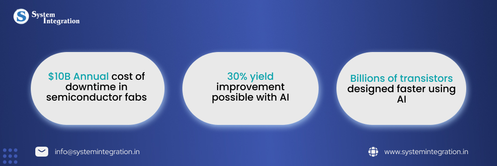
- Each wafer can cost upwards of $10,000 before packaging.
- Yield losses, machine downtime, or defects can bleed billions annually.
Traditional workflows rely on reactive problem-solving. Something breaks, engineers scramble, downtime occurs, and production halts. AI flips this around with predictive power: spotting issues before they happen and optimizing in real time.
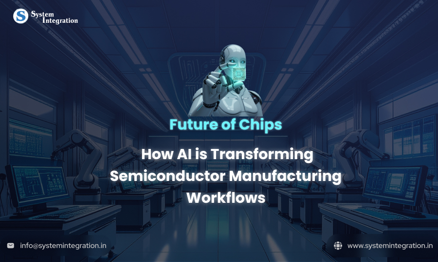
How AI is Transforming Semiconductor Manufacturing
AI powered Yield Optimization
Defects in semiconductor wafers are like bad apples in a basket, except these apples cost thousands. AI algorithms analyze inspection data at the microscopic level, identifying patterns that human eyes simply can’t.
Just like, Applied Materials claims AI-driven analytics can improve yields by up to 30% in certain fabs.
Predictive Maintenance = No More “Oops, Machine Down”
Equipment breakdown in a fab isn’t just an inconvenience—it’s a million-dollar nightmare. AI uses sensor data (temperature, vibration, acoustic signals) to predict failures before they occur.
- Before AI: A machine goes down → chaos → delayed shipments.
- After AI: AI flags unusual signals → scheduled maintenance → no surprises.”
AI in Design & Simulation
Modern chips pack billions of transistors. Designing them isn’t something you solve with coffee and a whiteboard. AI accelerates simulation, optimization, and layout verification—shrinking design cycles from months to weeks.
Defect Detection & Quality Assurance
AI-driven computer vision systems now scan wafers at lightning speed. Unlike humans, they don’t get tired, don’t blink, and definitely don’t complain about the night shift.
Workflow Automation in the Cleanroom
From scheduling machines to routing wafers, AI automates mundane but critical tasks. Think of it as the fab’s invisible project manager—efficient, precise, and without the office gossip.
Benefits of AI-Driven Semiconductor Workflows
- AI increases yields by producing more usable chips per wafer, directly improving profitability.
- Predictive maintenance reduces downtime by identifying potential equipment failures before they occur.
- Faster design and R&D cycles help companies bring new chips to market more quickly.
- Operational costs are lowered as AI optimizes resources and minimizes production waste.
- Sustainability is improved because AI-driven processes use less energy and reduce raw material consumption.
AI Fact Check
Did you know? A single 300mm wafer can hold over 100,000 chips.
Challenges to Watch Out For
- Implementing AI in semiconductor fabs requires high initial investment, making it costly for many manufacturers.
- The industry faces data overload, as cleaning and processing the enormous volume of fab data remains a major challenge.
- There is a skills gap since many engineers lack the expertise to fully leverage AI technologies.
- Integrating AI with existing legacy systems can be complex and time-consuming, often slowing adoption.
Future Outlook: Chips Making Chips?
The future points toward fully autonomous fabs where AI doesn’t just assist, it leads. Imagine a factory where machines self-correct, optimize in real-time, and even design next-gen chips themselves.
Are we talking about a future where chips design chips? Possibly. And when that happens, human engineers might finally get to take a proper lunch break.
“AI doesn’t get tired during the night shift, unlike humans and coffee machines.”
FAQs
AI is used for yield improvement, predictive maintenance, defect detection, workflow scheduling, and chip design optimization.
Not yet. AI assists by handling repetitive, data-heavy tasks, but human expertise is still crucial for strategic decisions and innovation.
Higher yields, reduced downtime, faster design cycles, and cost efficiency.
Yes, but long-term savings in yield, downtime, and efficiency outweigh the initial costs.